
 Home
>
products
>
Copper PCB
>
Home
>
products
>
Copper PCB
>
|
| Place of Origin | China |
| Brand Name | Customized |
| Certification | UL,ISO9001 |
| Model Number | Copper pcb board |
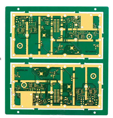
Buried copper" in PCB (Printed Circuit Board) technology:
"Buried copper" refers to a specific type of copper layer arrangement within a PCB.
In PCB manufacturing, copper layers are typically used for conducting electrical signals and providing connectivity between components. A standard PCB stackup consists of alternating layers of copper and insulating material, such as fiberglass epoxy.
In the case of buried copper, one or more additional copper layers are added between the standard copper layers. These extra copper layers are buried within the circuits pcb stackup and are not exposed on the outer layers.
The buried copper layers can be used for various purposes, such as power distribution, ground planes, or signal routing. By adding buried copper layers, the PCB designer can achieve better control over impedance, reduce electromagnetic interference (EMI), and improve signal integrity.
The buried copper layers are typically created during the pcb board fabrication process by laminating multiple copper-clad panels together with the insulating layers in between. The copper layers are etched and patterned to form the desired circuit traces and connections.
It's worth noting that implementing buried copper layers adds complexity and cost to the PCB manufacturing process. Therefore, it is commonly used in PCB designs with specific requirements for high-speed signals, controlled impedance, or EMI considerations.
CONTACT US AT ANY TIME

